Today’s PCB substrate is composed of a combination of CCL (Copper Clad Laminate, copper foil substrate) and PP (Prepreg, insulating film). CCL consists of three main components: Copper Foil, Reinforcement, and Epoxy resin. Since the advent of lead-free processes, a fourth component, Fillers, has been added to the PCB material to enhance its heat resistance.
To illustrate, envision Copper Foil as the veins in the human body, responsible for transporting vital blood, allowing the PCB to function. Reinforcement can be compared to the human skeleton, providing support and strength to prevent the PCB from becoming too flexible. Epoxy resin, in this analogy, represents the muscles, acting as the “fat” of the PCB.
Below, we will explain the uses, characteristics, and considerations of these four PCB materials:
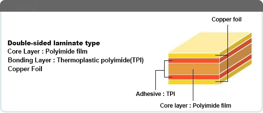
1.Copper Foil
- Electric Circuit: Conductive pathways.
- Signal line: Transmission lines for messages.
- Vcc: Power layer, operating voltage. As electronic products’ operating voltages have transitioned from 12V to 5V, 3V, and even 1V with technological advancements, the demand for high-quality Copper Foil has increased.
- GND (Grounding): Grounding layer. Think of Vcc as a water tower in a household; when we open the tap, water (electrons) flows out due to water pressure (operating voltage). GND can be likened to a drain, ensuring all used or excess water flows away; otherwise, flooding can occur in the house.
- Heat Dissipation (due to high thermal conductivity): Used for heat dissipation. Large copper areas are designed to release heat quickly into the air, preventing both human discomfort and electronic components from malfunctioning.
2.Reinforcement
- High Stiffness: Provides high rigidity, preventing PCB deformation.
- Dimension Stability: Maintains good dimensional stability.
- Low CTE: Low coefficient of thermal expansion, preventing internal circuit junctions from disconnecting and causing failure.
- Low Warpage: Exhibits low deformation, meaning low board bending or warping.
- High Modulus: High Young’s modulus.
3.Resin Matrix
- Heat Resistance: Excellent heat resistance ensures the board doesn’t delaminate after multiple heating and soldering processes.
- Low Water Absorption: Low water absorption prevents the main cause of PCB delamination.
- Flame Retardance: Must possess flame-retardant properties.
- Peel Strength: High tear strength.
- High Tg: High glass transition temperature. Materials with a high Tg are generally less water-absorbent, and this, not Tg alone, is fundamental in preventing delamination.
- Toughness: Good toughness or resistance to impact. Toughness is also known as “destructive energy,” and materials with higher toughness withstand impacts and damage better.
- Dielectric properties: High dielectric strength, indicating good insulating properties.
4.Fillers System

- Heat Resistance
- Low Water Absorption
- Flame Retardance
- High Stiffness
- Low CTE
- Dimension Stability
- Low Warpage
- Drill processability: Due to the high rigidity and toughness of fillers, PCB drilling can be challenging.
- High Modulus: Young’s modulus.
- Heat Dissipation (due to high thermal conductivity): Used for heat dissipation.
These characteristics play a crucial role in the design and manufacturing processes of PCBs.
For more information, please contact us.